
Fangyuan Meng 1,2,3Hongyan Yu 1,2,3Xuliang Zhou 1,2,3Mengqi Wang 1,2,3[ ... ]Jiaoqing Pan 1,2,3
Author Affiliations
Abstract
1 Key Laboratory of Semiconductor Materials Science, Institute of Semiconductors, Chinese Academy of Sciences, Beijing 100083, China
2 Center of Materials Science and Optoelectronics Engineering, University of Chinese Academy of Sciences, Beijing 100049, China
3 Beijing Key Laboratory of Low Dimensional Semiconductor Materials and Devices, Beijing 100083, China
A wide wavelength tuning range and single-mode hybrid cavity laser consists of a square Whispering-Gallery (WG) microcavity and a Fabry–Pérot (FP) was introduced and demonstrated. A wavelength tuning range over 12.5 nm from 1760.87 to 1773.39 nm which was single-mode emitting was obtained with the side-mode suppression ratio over 30 dB. The hybrid cavity laser does not need grating etching and special epitaxial structure, which reduces the fabrication difficulty and cost, and shows the potential for gas sensing with absorption lines in this range.
Journal of Semiconductors
2022, 43(6): 062302

Fangyuan Meng 1,2,3Hongyan Yu 1,2,3,*Xuliang Zhou 1,2,3,**Yajie Li 1,2,3[ ... ]Jiaoqing Pan 1,2,3
Author Affiliations
Abstract
1 Key Laboratory of Semiconductor Materials Science, Institute of Semiconductors, Chinese Academy of Sciences, Beijing 100083, China
2 Center of Materials Science and Optoelectronics Engineering, University of Chinese Academy of Sciences, Beijing 100049, China
3 Beijing Key Laboratory of Low Dimensional Semiconductor Materials and Devices, Beijing 100083, China
4 School of Physics, Peking University, Beijing 100871, China
Gas sensing for measurement of gas components, concentrations, and other parameters plays an important role in many fields. In this Letter, a micro-ring resonator laser used for gas sensing is experimentally demonstrated. The multi-quantum-wells micro-ring laser based on whispering-gallery modes with an annular resonator and an output waveguide was fabricated. A single-mode laser with a wavelength of 1746.4 nm was fabricated for the first time, to the best of our knowledge, experimentally. The output power of 1.65 mW under 40 mA injection current was obtained with a side-mode suppression ratio over 33 dB.
gas sensing whispering-gallery mode micro-ring resonator laser Chinese Optics Letters
2021, 19(4): 041406
Author Affiliations
Abstract
1 Key Laboratory of Semiconductor Materials Science, Institute of Semiconductors, Chinese Academy of Sciences, Beijing 100083, China
2 Center of Materials Science and Optoelectronics Engineering, University of Chinese Academy of Sciences, Beijing 100049, China
3 Beijing R&D Institute, VanJee Technology, Beijing 100193, China
A SiN-Si dual-layer optical phased array (OPA) chip is designed and fabricated. It combines the low loss of SiN with the excellent modulation performance of Si, which improves the performance of Si single-layer OPA. A novel optical antenna and an improved phase modulation method are also proposed, and a two-dimensional scanning range of is achieved, which makes the OPA chip more practical.
Photonics Research
2020, 8(6): 06000912

Wenyu Yang 1,2,3Yajie Li 1,2,3Fangyuan Meng 1,2,3Hongyan Yu 1,2,3[ ... ]Jiaoqing Pan 1,2,3
Author Affiliations
Abstract
1 Key Laboratory of Semiconductor Materials Science, Institute of Semiconductors, Chinese Academy of Sciences, Beijing 100083, China
2 Center of Materials Science and Optoelectronics Engineering, University of Chinese Academy of Sciences, Beijing 100049, China
3 Beijing Key Laboratory of Low Dimensional Semiconductor Materials and Devices, Beijing 100083, China
Silicon-based photonic integration has attracted the interest of semiconductor scientists because it has high luminous efficiency and electron mobility. Breakthroughs have been made in silicon-based integrated lasers over the past few decades. Here we review three main methods of integration of III–V materials on Si, namely direct growth, bonding, and selective-area hetero-epitaxy. The III–V materials we introduced mainly include materials such as GaAs and InP. The lasers are mainly lasers of related communication bands. We also introduced the advantages and challenges of the three methods.
Journal of Semiconductors
2019, 40(10): 101305
Yajie Li 1,2,3Hongyan Yu 1,2,3,4Wengyu Yang 1,2,3Chaoyang Ge 5[ ... ]Jiaoqing Pan 1,2,3,6
Author Affiliations
Abstract
1 Key Laboratory of Semiconductor Materials Science, Institute of Semiconductors, Chinese Academy of Sciences, Beijing 100083, China
2 Center of Materials Science and Optoelectronics Engineering, University of Chinese Academy of Sciences, Beijing 100049, China
3 Beijing Key Laboratory of Low Dimensional Semiconductor Materials and Devices, Beijing 100083, China
4 e-mail: hyyu09@semi.ac.cn
5 State Key Laboratory for Artificial Microstructure and Mesoscopic Physics, School of Physics, Peking University, Beijing 100871, China
6 e-mail: jqpan@semi.ac.cn
A 4–λ hybrid InGaAsP-Si evanescent laser array is obtained by bonding III–V distributed feedback lasers to a silicon on insulator (SOI) substrate using a selective area metal bonding technique. Multiple wavelengths are realized by varying the width of the III–V ridge waveguide. The threshold current is less than 10?mA for all wavelength channels under continuous-wave (CW) operation at room temperature, and the lowest threshold current density is 0.76??kA/cm2. The side mode suppression ratio (SMSR) is higher than 40?dB for all wavelength channels when the injection current is between 20?mA and 70?mA at room temperature, and the highest SMSR is up to 51?dB. A characteristic temperature of 51?K and thermal impedance of 144°C/W are achieved on average. The 4–λ hybrid InGaAsP-Si evanescent laser array exhibits a low threshold and high SMSR under CW operation at room temperature. The low power consumption of this device makes it very attractive for on-chip optical interconnects.
Photonics Research
2019, 7(6): 06000687

Author Affiliations
Abstract
1 Key Laboratory of Semiconductor Materials Science, Beijing Key Laboratory of Low Dimensional Semiconductor Materials and Devices, Institute of Semiconductors, Chinese Academy of Sciences, Beijing 100083, China
2 College of Materials Science and Opto-Electronic Technology, University of Chinese Academy of Sciences, Beijing 100049, China
A monolithic integrated few-mode transmitter comprising of two directly modulated distributed feedback lasers and a multimode-interference-coupler-based mode converter-multiplexer with 66% mode conversion efficiency was designed and demonstrated. A fundamental TE0 mode and a first-order TE1 mode were successfully generated from the transmitter, with the output power of 4 and 5.5 mW at a pump current of around 150 mA, respectively, at the common output port. The small signal modulation bandwidth of the TE0 and TE1 channels reached 17.4 and 14.7 GHz, respectively. Error-free 2×10-Gbit/s direct modulation of the two-mode transmitter was demonstrated, with a power penalty of 4.3 dB between the TE0 mode and the TE1 mode at the bit error rate of 1×10 9.
Multiplexing Optical interconnects Photonic integrated circuits Semiconductor lasers Photonics Research
2018, 6(5): 05000463
1 中国科学院半导体研究所半导体材料科学重点实验室, 低维半导体材料与器件北京市重点实验室, 北京 100083
2 北京大学物理学院人工微结构和介观物理国家重点实验室, 北京 100871
3 格拉斯哥大学物理学院, 格拉斯哥G12 8LT, 英国
采用两段式被动锁模激光器结构, 利用隧道结级联两组量子阱有源区, 实现了一种工作在近红外波段的单片集成大功率量子阱被动锁模激光器。对该锁模激光器的锁模特性进行了表征, 测试得到该锁锁模激光器工作中心波长为1038 nm, 激光脉冲重复频率为24.37 GHz, 改变激光器的工作条件, 其脉冲宽度变化范围为2.19~9.27 ps, 峰值功率变化范围为76~308 mW, 表明该锁模激光器具有单片集成、体积小、功率大、重复频率高等优良特性。同时, 在一定的反向偏压条件下, 该锁模激光器呈现出功率双稳态的特性, 扩大了有效锁模范围。
激光器 锁模激光器 半导体激光器 多量子阱 超快激光
Author Affiliations
Abstract
1 Key Laboratory of Semiconductor Materials Science and Beijing Key Laboratory of Low Dimensional Semiconductor Materials and Devices, Institute of Semiconductors, Chinese Academy of Sciences, Beijing 100083, China
2 Network Technology Research Institute, China United Network Communications Corporation Limited, Beijing 100048, China
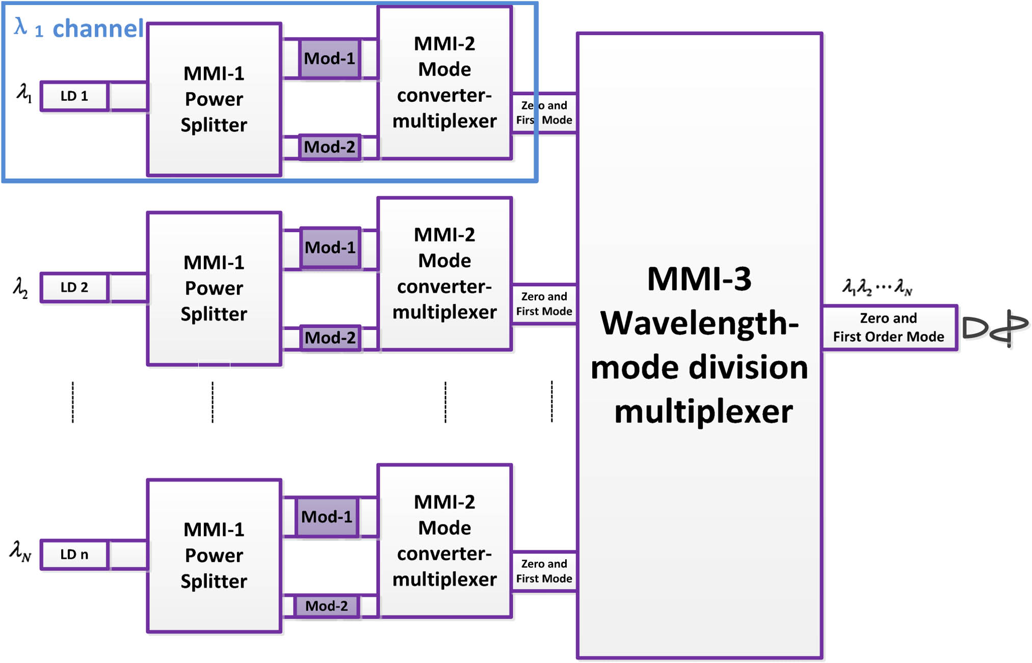
An InP-based monolithically integrated few-mode transmitter aiming at the combination of wavelength division multiplexing (WDM) and mode division multiplexing (MDM) technologies is proposed. The core elements of the proposed transmitter are mode converters and a wavelength-mode division multiplexer that are all based on multimode interference (MMI) couplers. Simulations show that the wavelength-mode division multiplexer has a large fabrication tolerance of 30 and 0.5 μm for the length and the width of the device, respectively. A low loss below 0.26 dB for the passive parts of the transmitter is obtained in the whole C-band wavelength range.
250.5300 Photonic integrated circuits 060.4230 Multiplexing 060.4510 Optical communications Chinese Optics Letters
2016, 14(8): 080601


